News Story
Leite to Lead Solar Tutorial at APS Physics Conference
The 2016 American Physical Society (APS) March Meeting will bring together nearly 10,000 scientists from around the world to share groundbreaking research from universities and other research institutions. This year, APS will feature a series of tutorials on the exciting new developments of a variety of topics.
Professor Marina Leite, from the Dept. of Materials Science & Engineering (MSE) and the Institute for Research in Electronics & Applied Physics (IREAP), will lead Tutorial #2: Probing Photovoltaic Devices with State-of-the-Art Imaging Tools. She is teaming up with colleagues from Lund University in Sweden, John Hopkins University and Arizona State University to discuss the latest advancements in photovoltaics.
Detailed information about the tutorial can be found below. Visit the APS website to register to attend, online registration closes this Friday, February 12th, but attendees will be able to register onsite.
Location and date:
Baltimore Convention Center, room TBD
Sunday, March 13, 2016, 8:30 a.m. - 12:30 p.m.
Audience:
Graduate students, postdocs, and researchers interested in an introduction to modern characterization tools for renewable energy devices, from their instrumentation to data interpretation.
Organizer: Marina Leite, University of Maryland
Instructors (alphabetical order):
• Mariana Bertoni, Arizona State University
• Knut Deppert, Lund University, Sweden
• Marina Leite, University of Maryland, College Park
• Susanna Thon, John Hopkins University
Description of tutorial:
This tutorial aims at discussing the latest advancements on photovoltaics, including fundamental physical phenomena to advance the understanding of the mesoscale behavior of emerging materials for PV. State-of-the-art, modern tools that are currently used to image photovoltaic devices with unprecedented spatial resolution will be introduced. The series of four lectures will include: (i) a review of the latest advancements of the different PV technologies; (ii) an overview of how wire geometries are implemented as PV devices; (iii) the different probes used to characterize PV materials, including electron beam, X-rays, and near-field scanning optical microscopy, and how they are implemented to provide new information related to the optoelectronic response of the devices; (iv) how sophisticated instrumentation can pave the way for advancing our understanding of light-matter interactions in photovoltaic devices.
Published February 9, 2016
Recent Stories
Stories / Apr 19, 2024
CEEE Publishes Paper About “Cool” Technology
Stories / Apr 3, 2024
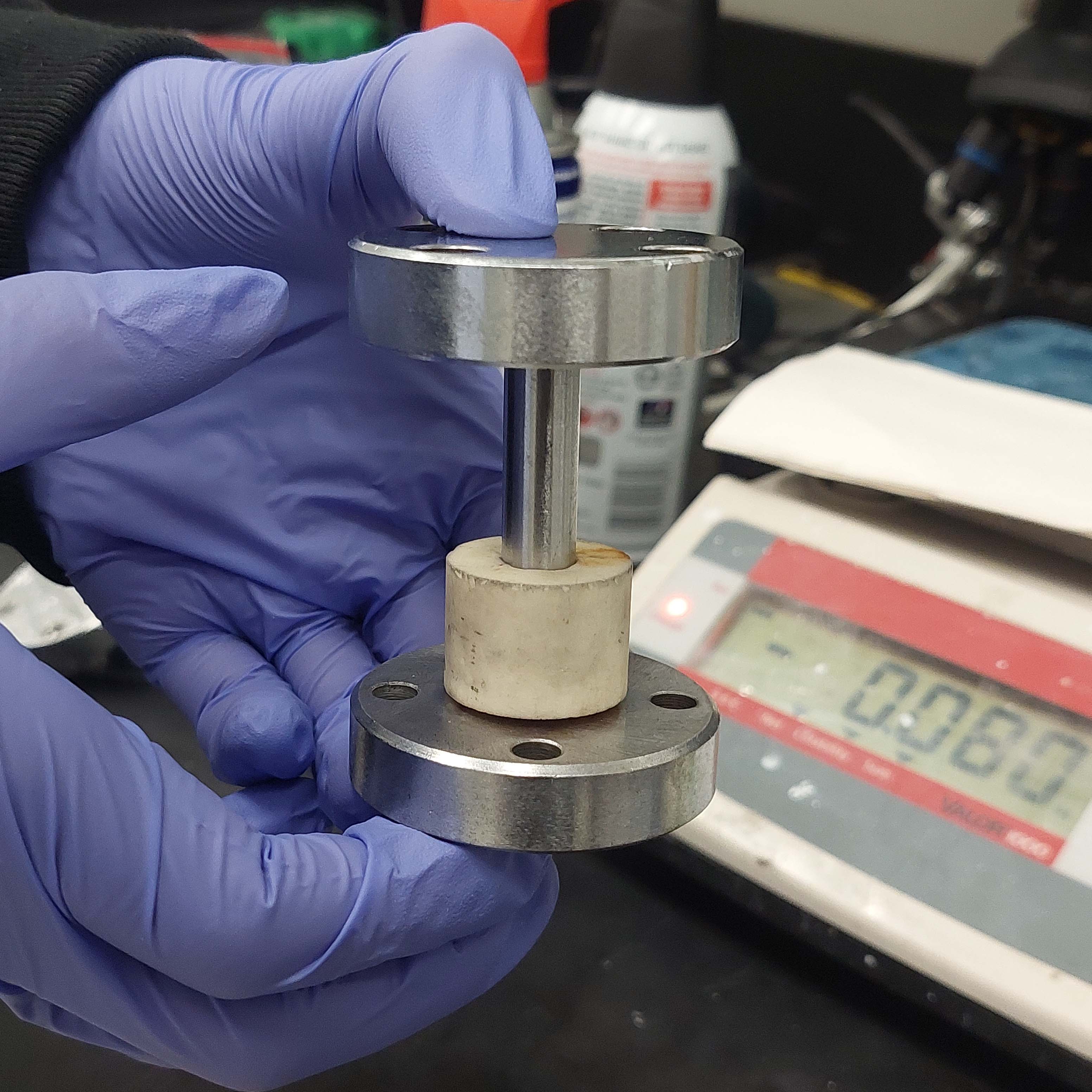
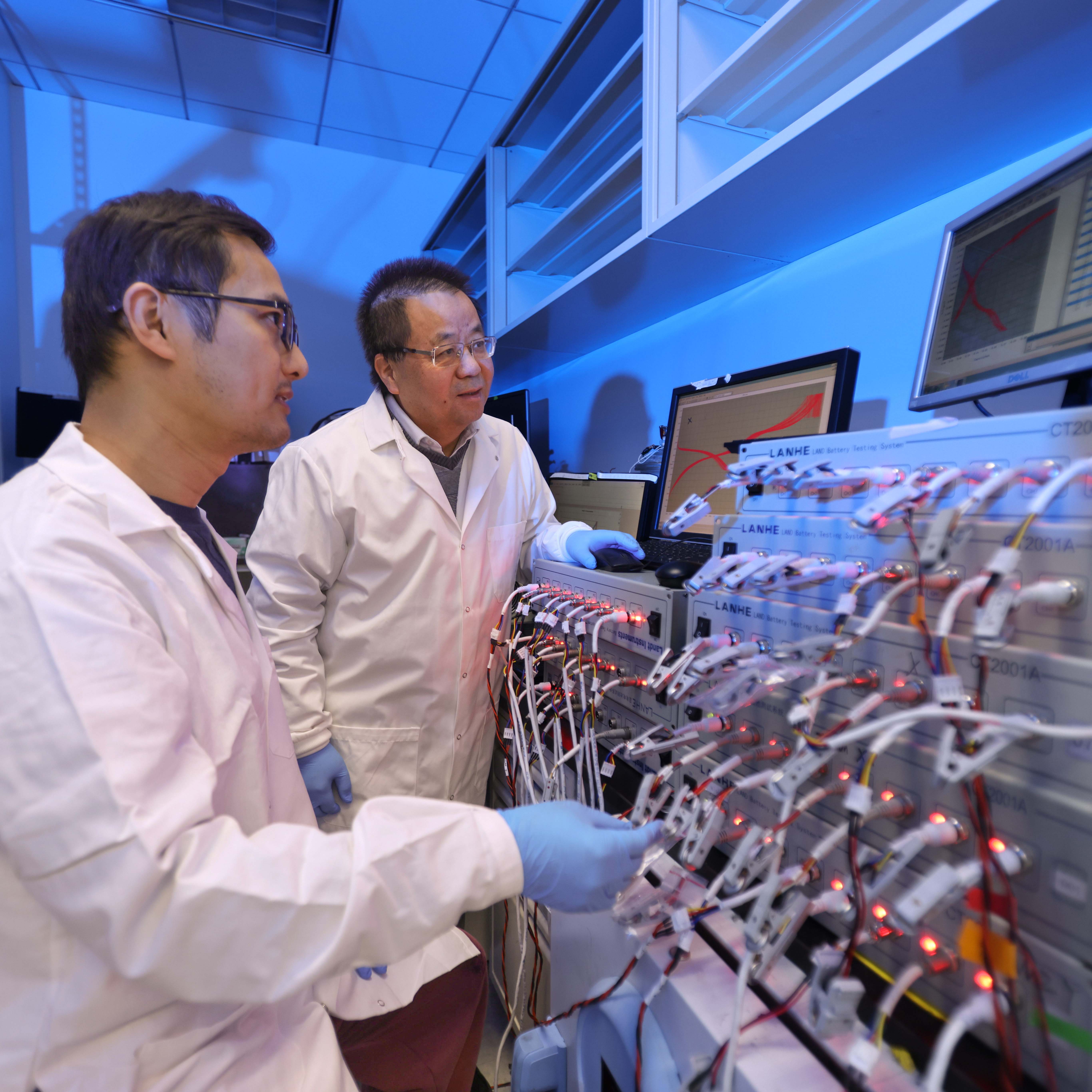
Next-Generation Batteries Could Come with Lower Production...
Stories / Mar 26, 2024
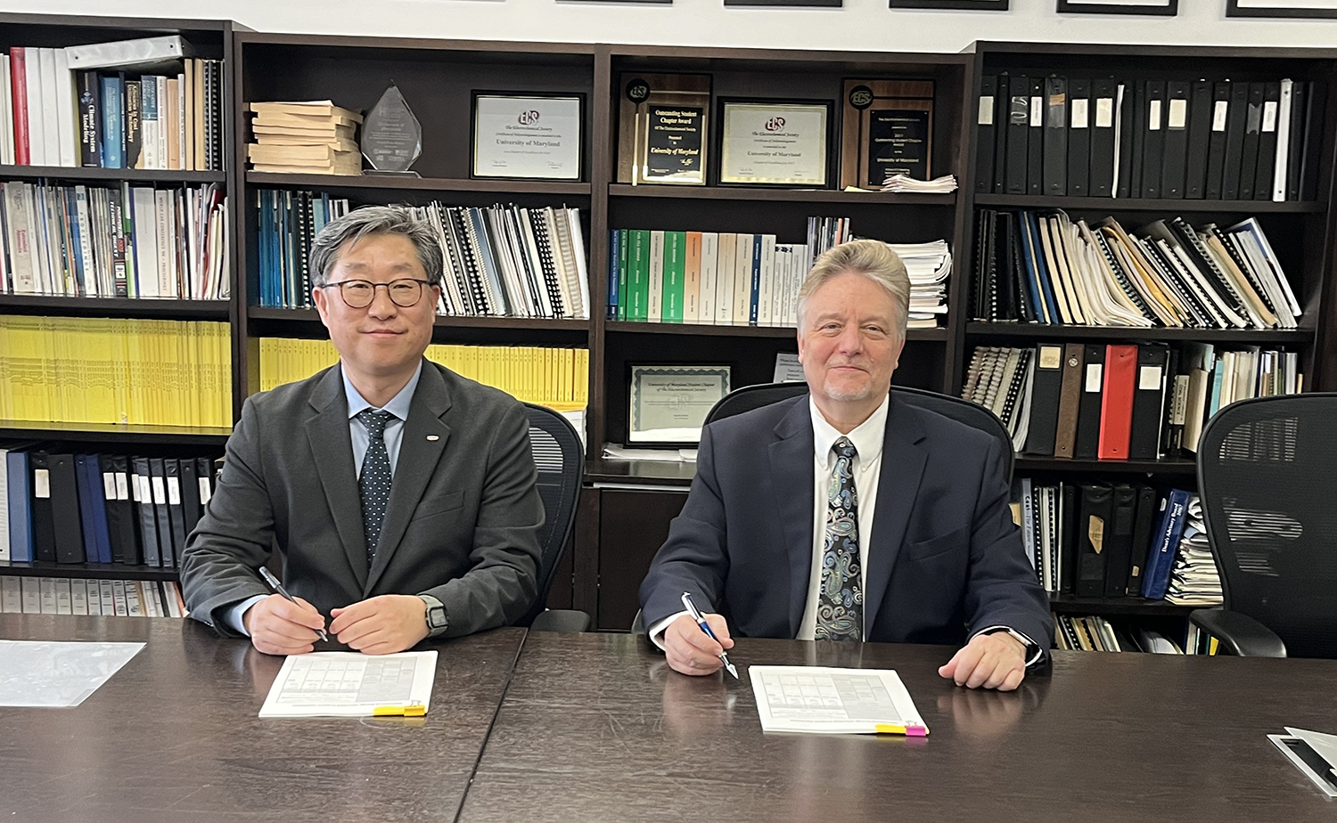
International Energy Cooperation Center Established at...
Stories / Mar 26, 2024
Maryland Researchers Awarded $1.5 Million to Pioneer Batteries...

Stories / Mar 25, 2024
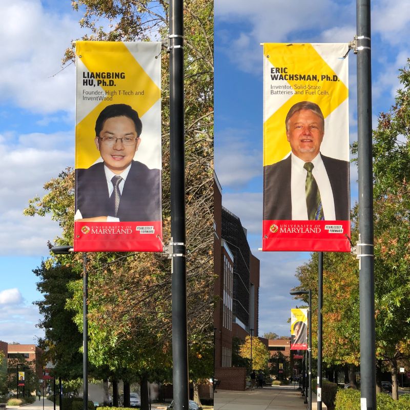
Liangbing Hu and Eric Wachsman Graced UMD’s Innovation Gateway
Stories / Feb 26, 2024
$15 Million Climate Catalytic Capital Fund Launched
Stories / Feb 9, 2024
Twisting & Shouting for Clean Energy
Stories / Jan 17, 2024
$15M Federal Grant Awarded to Support Maryland Electric Vehicle...

Stories / Jan 12, 2024
Lighter, Safer and Stronger Batteries Could Power the Smart...
Stories / Jan 9, 2024
Safer Electric Vehicles Could Come Soon After this Recent...